 |
| April 24, 2012 | Volume 08 Issue 16 |
Designfax weekly eMagazine
Archives
Partners
Manufacturing Center
Product Spotlight
Modern Applications News
Metalworking Ideas For
Today's Job Shops
Tooling and Production
Strategies for large
metalworking plants
Tiny MEMS chips go 3D

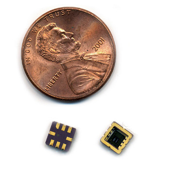
A new approach helps researchers make tiny three-dimensional structures. Pictured are two packaged microchips (enlarged), each with tiny bridges fabricated on their surfaces.
MIT researchers develop a new approach to producing three-dimensional microchips.
By Jennifer Chu, MIT
Microelectromechanical systems, or MEMS, are small devices with huge potential. Typically made of components less than 100 microns in size the diameter of a human hair they have been used as tiny biological sensors, accelerometers, gyroscopes, and actuators.
For the most part, existing MEMS devices are two-dimensional, with functional elements engineered on the surface of a chip. It was thought that operating in three dimensions to detect acceleration, for example would require complex manufacturing and costly merging of multiple devices in precise orientations.
Now researchers at MIT have come up with a new approach to MEMS design that enables engineers to design 3D configurations, using existing fabrication processes; with this approach, the researchers built a MEMS device that enables 3D sensing on a single chip. The silicon device, not much larger than Abraham Lincoln's ear on a U.S. penny, contains microscopic elements about the width of a red blood cell that can be engineered to reach heights of hundreds of microns above the chip's surface.
Fabio Fachin, a postdoc in the Department of Aeronautics and Astronautics, says the device may be outfitted with sensors, placed atop and underneath the chip's minuscule bridges, to detect three-dimensional phenomena such as acceleration. Such a compact accelerometer may be useful in several applications, including autonomous space navigation, where extremely accurate resolution of three-dimensional acceleration fields is key.
"One of the main driving factors in the current MEMS industry is to try to make fully three-dimensional devices on a single chip, which would not only enable real 3D sensing and actuation, but also yield significant cost benefits," Fachin says. "A MEMS accelerometer could give you very accurate acceleration [measurements] with a very small footprint, which in space is critical."
Fachin collaborated with Brian Wardle, an associate professor of aeronautics and astronautics at MIT, and Stefan Nikles, a design engineer at MEMSIC, an Andover, MA, company that develops wireless-sensor technology. The team outlined the principles behind their 3D approach in a paper accepted for publication in the Journal of Microelectromechanical Systems.
Moving to 3D
While most MEMS devices are two-dimensional, there have been efforts to move the field into 3D, particularly for devices made from polymers. Scientists have used lithography to fabricate intricate, three-dimensional structures from polymers, which have been used as tiny gears, cogs, and micro-turbines. However, Fachin says, polymers lack the stiffness and strength required for some applications, and can deform at high temperatures qualities that are less than ideal in applications like actuators and shock absorbers.
By contrast, materials such as silicon are relatively durable and temperature resistant. But, Fachin says, fabricating 3D devices in silicon is tricky. MEMS engineers use a common technique called deep reactive ion etching to make partially 3D structures, in which two-dimensional elements are etched into a wafer. The technique, however, does not enable full 3D configurations, where structures rise above a chip's surface.
To make such devices, engineers fabricate tiny two-dimensional bridges, or cantilevers, on a chip's surface. After the chip is produced, they apply a small force to arch the bridge into a three-dimensional configuration. This last step, Fachin says, requires great precision.
Inner stress
Instead, the MIT team came up with a way to create 3D MEMS elements without this final nudge. The group based its approach on residual stress: In any bridge structure, no matter its size, there exist stresses that remain in a material even after the original force needed to produce it such as the heat or mechanical force of a fabrication process has disappeared. Such stresses can be strong enough to deform a material, depending on its dimensions.
Fachin and his colleagues studied previous work on microbeam configurations and developed equations to represent the relationship between a thin-film material's flexibility, geometry, and residual stress. The group then plugged their desired bridge height into the equations and came up with the amount of residual stress required to buckle or bend the structure into the desired shape. Fachin says other researchers can use the group's equations as an analytical tool to design other 3D devices using pre-existing fabrication processes.
"This offers a very cost-effective way for 3D structures," says Y.K. Yoon, an associate professor of electrical and computer engineering at the University of Florida who did not take part in the research. "Since the process is based on a silicon substrate, and compatible with standard complementary metal oxide semiconductor (CMOS) processes, it will also offer a pathway to a smart CMOS-MEMS process, with good manufacturability."
The group used their analytical tool to design tiny 3D devices out of a composite silicon structure, with each chip containing highly curved or buckled microbeams. Fachin's sensors, placed on top of each bridge and on the surface of the chip, can triangulate to measure acceleration.
"For other applications where you want to go much larger in size, you could just pick a material that has a larger residual stress, and that would cause the beam to buckle more," Fachin says. "The flexibility of the tool is important."
Published April 2012
Rate this article
View our terms of use and privacy policy
